


Author: Site Editor Publish Time: 2025-12-08 Origin: Site


This guide concerns cell interconnection. Review candidate short-wave emitters and medium-wave emitters against the qualified process; no generic temperature or distance is a production recommendation.
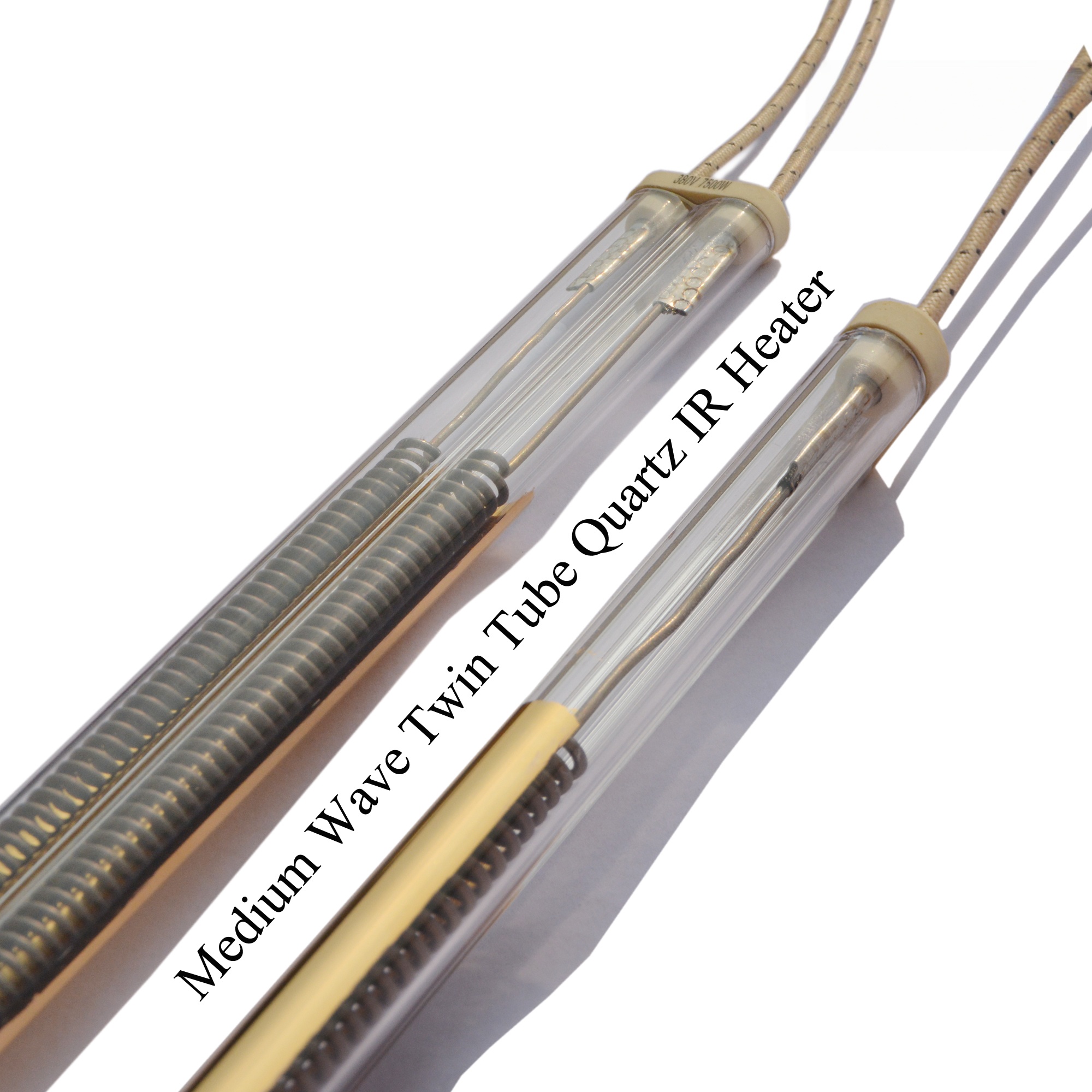
Emitter construction example, not a qualified PV soldering recipe.
Quartz infrared lamps can provide non-contact heat in a suitably engineered tabber-stringer installation. Validate where the energy is absorbed and the resulting thermal profile.
This article looks at solar wafer soldering from a process engineer’s point of view: how the line runs, where heat is required, how quartz IR can be integrated or retrofitted, what kind of configurations are realistic, and where IR is – and is not – the right tool.
In a standard crystalline silicon module line, the cell interconnection process typically includes:
Load and inspect the specified cell format and thickness, including handling and crack-control requirements.
Flux application
– Flux is applied to the busbars or pads on the cell surface and sometimes to the copper ribbons to promote solder wetting and oxide removal.
Ribbon placement and alignment
– Tinned copper interconnect ribbons are positioned onto the busbars by the tabber-stringer machine, often under vacuum or mechanical support.
Soldering / bonding (tabbing & stringing)
– Heat is applied to reflow the solder coating on the ribbon (and sometimes additional solder paste) to form a metallurgical joint with the cell busbar.
Cooling and string handling
– The joint is cooled in a controlled way while the string is transported, then strings are laid up for bussing and lamination.
Throughout this sequence, heating is concentrated in the soldering zone, but preheating and controlled cooling are also critical to avoid thermal shock and mechanical stress on thin wafers.
Key locations where precise heating is required:
Bring cells and interconnects through the preheat stage specified by the qualified soldering process.
Raise the solder interface through the alloy-specific reflow profile, while respecting the cell and metallization thermal limits.
Post-solder thermal conditioning
– Avoiding abrupt cooling that can induce microcracks or warpage, especially with larger/thinner cells.
Excessive thermal variation can contribute to:
Incomplete solder wetting or “cold” joints.
Local overheating, discoloration, or microcracks.
Lower string yield and higher rework/scrap.
Many tabber-stringer lines in the field still rely on older or mixed heating technologies. The most common are:
Contact soldering tips / shoes
Heated belts or hot plates
Hot air or convection tunnels
Conventional IR panels with slow response
Each has characteristic limitations in the context of high-throughput, high-precision PV cell soldering.
Contact tools apply heat by conduction. Typical issues:
Mechanical stress and risk of cracking
– Even finely controlled pressure can stress thin wafers, especially with small non-planarities or foreign particles.
Non-uniform contact
– Slight variations in planarity or contamination cause local under- or over-heating.
Slow thermal response
– Large metal masses are slow to heat and cool, making it difficult to adjust the temperature profile quickly for new products or recipes.
Maintenance and contamination
– Solder build-up and flux residues require regular cleaning, which impacts uptime.
Hot air or convection systems heat both the product and surrounding air:
Low energy efficiency
– Much of the energy goes into heating air and metal fixtures rather than the ribbons and cells.
Limited local control
– It is difficult to create sharp temperature peaks or narrow zones; heat spreads beyond the target region.
Potential for flux disturbance
– Airflow can disturb flux distribution or introduce contamination.
Some lines use older IR panels with ceramic emitters or slow-response lamps:
Slow response to setpoint changes
– Not ideal for fast recipe changes or dynamic power modulation.
Limited zoning
– Coarse zoning may not match modern multi-busbar or multi-wire layouts.
Size and footprint
– Larger furnaces occupy more line length, which conflicts with compact, high-throughput layout requirements.
These limitations have driven many engineers and machine builders to adopt quartz infrared heating lamps as the primary or supplemental heat source in modern soldering zones.
Quartz IR lamps deliver intense, radiant energy directly to the cell and ribbon surfaces without physical contact. In PV soldering lines, they are typically integrated in three roles: preheating, boosting, and full IR soldering.
An IR preheating module is usually placed just before the main soldering point:
Bring cells and interconnects through the preheat stage specified by the qualified soldering process.
Implementation
– An appropriately sized array of quartz infrared lamps above (and sometimes below) the transport path.
– Zoning along the direction of travel to shape a gentle temperature ramp.
Preheating with IR is particularly effective when retrofitting older lines that run close to their temperature limit and struggle with scrap due to cracking.
Instead of relying solely on contact tips or hot plates, many modern designs use IR to provide the sharp reflow peak:
Boost from below or above
– Lamps are positioned to focus on the busbar/ribbon area while minimizing heating of non-critical regions.
Synchronized with mechanical tools
– IR power is ramped up exactly when ribbons are pressed, then reduced during release and cooling.
A hybrid design may retain existing tooling; validate its thermal profile and cycle time on the actual machine.
In new-build tabber-stringer lines, quartz IR lamps can fully replace traditional heating:
All-IR soldering heads
– Arrays of lamps, often with reflectors and focusing optics, deliver precisely shaped heating patterns to each busbar or wire layout.
Top and bottom heating
– Cells can be heated from both sides to improve uniformity and to compensate for varying ribbon cross-sections.
Independent zones
– Each zone (preheat, reflow, post-heat) is independently controlled, enabling fine tuning for different cell sizes and solder recipes.
This approach eliminates direct mechanical heating, lowers moving mass in the head, and simplifies temperature control logic.
Use the cell supplier, interconnection material and machine process requirements to define the allowed thermal profile. Preheat, peak temperature, time above liquidus and cooling limits cannot be transferred automatically between solder alloys, cell constructions or ribbon layouts.
| Input | Confirm before design |
|---|---|
| Cell and interconnect | Cell technology, thickness, metallization, ribbon or wire and solder/flux system. |
| Thermal requirement | Qualified ramp, peak, hold and cooling profile at the relevant location. |
| Motion | Indexing or continuous transport, available heating time and target output. |
| Optical geometry | Lamp orientation, distance, reflectors, supports and shaded regions. |
| Measurement | Sensor suitability, emissivity/reflection effects and a correlated reference method. |
| Acceptance | Joint integrity, electrical performance, damage inspection and repeatability. |
Electrical power divided by lamp area is not the same as incident radiation at the cell or absorbed power in the joint. Define the measurement basis when comparing power density. Determine lamp number and spacing through the qualified thermal requirement and trials.
Mounting distance must accommodate coverage, cell supports, camera and handling access, thermal expansion and maintenance. Treat any supplier example as a test candidate rather than a production recipe.
Compare the proposed installation with the existing process using the same cell, interconnect materials and acceptance criteria. Record thermal profiles, joint pull-test results, crack inspection, electrical performance, accepted output and total process energy.
Infrared heating may reduce unnecessary heating of surrounding equipment, but savings and cycle-time changes are installation-specific. Include auxiliary loads, idle periods and rejected material. A faster lamp response does not guarantee higher yield or a shorter qualified soldering cycle.
To get the best results from quartz IR modules, several PV-specific design and tuning aspects must be considered.
Silicon wafers, anti-reflective coatings, solder alloys, and copper ribbons each have different absorption spectra.
Short-wave IR tends to penetrate deeper and can heat both the ribbon and the cell; medium-wave often couples more strongly to certain surfaces and coatings.
In practice, many PV lines use short-wave lamps for the main soldering zone, where aggressive response is desired, and may use medium-wave or lower power for preheat or post-heat zones.
A short feasibility study with actual wafers and ribbons is usually the most efficient way to choose.
Shiny copper ribbons and busbars can reflect IR, causing hot spots if not managed:
Use appropriate reflector geometry (gold, white ceramic, or polished metal) to redirect stray radiation back into useful areas rather than onto sensitive components.
Tilt lamp and reflector assemblies slightly to avoid concentrating reflections at cell edges or corners.
Consider selective shielding where cameras or plastic parts might otherwise see high radiation levels.
A robust soldering profile typically:
Gradually ramps cell temperature in the preheat zone.
Delivers a sharp but controlled reflow peak over a short time.
Allows controlled cooling without sudden quenching.
This can be achieved by:
Configuring multiple zones with stepped power levels instead of a single uniform zone.
Using conveyor speed and lamp power together to tune the time-temperature curve.
Monitoring reference cells/strings with thermocouples or IR pyrometers during commissioning.
For high-end lines, integrating temperature feedback improves robustness:
Attach thermocouples to representative dummy cells or strings at known positions.
Use pyrometers or IR cameras for non-contact monitoring in critical zones.
Feed this information into the IR power control to compensate for ambient variations or lamp aging.
Quartz IR lamps are consumables in a high-duty environment:
Design modules for quick lamp replacement with accessible connectors and guides.
Plan regular cleaning (dust, flux fumes) to maintain efficiency and uniformity.
Track lamp operating hours and power levels to schedule preventive replacement before performance drifts outside the process window.
Even experienced teams can run into recurring issues when adding or upgrading IR modules. Some typical pitfalls include:
If IR heaters are too narrowly focused over the busbar area:
The ribbon and busbar may reach the target solder temperature.
Cell edges remain significantly cooler, leading to partial wetting or weak joints near the cell perimeter.
Mitigation:
Use wider or carefully profiled heating patterns that cover the entire busbar width plus a margin.
Balance top and bottom heating so the complete joint area, not just the top surface, reaches the required temperature.
Driving the reflow zone too hard, or keeping cells above liquidus for too long, can:
Damage anti-reflective coatings.
Cause warpage or microcracks, especially in thin large-area cells.
Accelerate degradation of neighboring materials.
Mitigation:
Validate the complete time-temperature profile with test cells, not just surface temperature readings.
Tune down peak power and/or shorten dwell time while checking solder joint quality (pull tests, cross-sections).
Without careful design:
Reflected IR can hit plastic covers, cables, or sensor housings, causing local overheating.
Cameras or optical sensors may be blinded or thermally stressed.
Mitigation:
Incorporate shields and baffles as part of the IR module design.
Verify during commissioning with temperature labels or thermal imaging.
In retrofit projects, it is common to size IR modules based on current operating speeds only:
When production later attempts to increase line speed, the installed power may be insufficient to maintain the same profile.
Mitigation:
Size lamp arrays with headroom for future speed increases (based on the agreed future throughput and validated thermal load).
Design control systems so that extra power is available but only used when needed.
Standard SMT or wave soldering logic does not always translate directly to PV:
Cells are larger, thinner, and more fragile.
The mechanical support/deformation behavior is different.
Optical and thermal properties of the stack differ from typical PCB assemblies.
Mitigation:
Base design decisions on PV-specific tests and data, not only on general electronics experience.
Involve PV process engineers early when specifying IR modules.
Provide cell and ribbon details, solder and flux specifications, the qualified thermal profile, machine sequence and existing lamp data. Define whether the request is an equivalent replacement, a controlled retrofit or a new module design. Agree on testing, documentation, integration and support responsibilities for the specific project.
No. The solder alloy, cell technology, metallization and interconnect define the allowed process.
No. Correlate the measurement method to the relevant joint and cell temperature.
No. Geometry, motion, controls, cooling and process qualification need review.
Send the machine model, original lamp data and qualified thermal profile for a PV heating review.
Last updated: September 8, 2026


